m9b · part 3 of 6
Two PSRAM dies, one memory
Everything the CPU runs, and every pixel and sample the display gets, comes out of the two PSRAM dies in the package. On paper they deliver 664 MB/s. The CPU gets a few percent of that, and this part is about why, and what that means for the design.
The bus
Each of the two 32 Mbit dies has a HyperBus-style interface: eight data lines (DQ) used on both clock edges, a differential clock, a chip select, and a strobe called RWDS. A transfer goes like this:
- Command: six bytes that say read or write, and where. On a double-data-rate bus that’s three clocks.
- Latency: the die makes you wait. m9b configures it for a fixed latency of 6 clocks, doubled: 12 clocks of nothing.
- Data: a byte on every clock edge, for as long as chip select stays low.
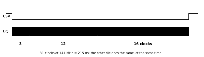
So a transfer has a fixed cost up front, and after that it’s cheap. Fetch one word, and you pay the whole setup for four bytes. Fetch a 64-byte line, and the setup is shared across all of it. That’s why the CPU’s caches move whole lines, and why the video engine fetches in 256-byte blocks.
The dies have no linear burst mode, only bursts that wrap within a configured length. m9b sets 128 bytes per die (configuration register CR0 = 0x8f1c, written about 200 µs after reset). A cache line, 32 bytes per die and aligned, never reaches the wrap, and the controller ends it early by raising chip select. A DMA block is exactly one full wrap: 128 bytes per die, 256 in all.
Two dies in lockstep
The controller drives both dies with the same command, address and timing, each on its own data bus. Every 72 MHz controller cycle moves 32 bits per die, 64 bits in all: even 32-bit words live in die 0, odd ones in die 1. To everything else in the system, that’s one 8 MB memory with a 16-bit double-data-rate bus.
That’s where the headline number comes from: 166 MHz × 2 edges × 2 dies = 664 MB/s at the dies’ rated clock. m9b runs them at 144 MHz, so 576 MB/s.
The PHY
The FPGA fabric can’t toggle pins at 144 MHz double data rate from plain logic. Each PSRAM pin goes through the chip’s hard I/O blocks instead: an OSER4 serializer takes four bits from the controller per 72 MHz cycle and shifts them out on both edges of the 144 MHz clock; an IDES4 deserializer does the reverse for reads.
Reads are the hard direction. The data comes back aligned to the die’s own view of the clock, after delays through the package and the pins, and the FPGA has to sample each bit in the middle of its window. Both the outgoing clock and the incoming data go through programmable delay lines (IODELAY). I swept the two delays in simulation and on the board, and picked the middle of the window that worked when the board was initially brought up at 148.5 MHz (that was an early version of the video hardware that still tried to do 720p, which has a dot clock of 74.25MHz, so the RAM was running at twice that). That delay also worked at 162 MHz, and at today’s 144 MHz. The read stream arrives skewed by one byte, and the controller reassembles each 32-bit word from two consecutive cycles. On typical RAM controllers, this delay is continuously calibrated and adjusted, which costs a lot of logic - using a fixed precalibrated delay is the secret to keeping the controller small. I tested on multiple boards in various conditions to convince myself it is reasonably stable.
The other trick is using the same controller across both dies, although there is a hefty price to pay for that: the two dies are independent, and may thus refresh at different times. The only way to not have to account for refreshes is to choose the fixed latency mode, which costs an extra 6 cycles on every access where no refresh is happening (which would be most of them).
Who gets the bus
Two kinds of client share the controller:
- Cache lines, from the CPU: a refill (read a 64-byte line) or a write-back (write a dirty one). The CPU is stalled on them, so they go first.
- DMA, from the video engine: a video line (up to 1,440 bytes) or an audio block (1 KB) copied into the transfer RAM, the on-chip buffer the video side reads from. These come in 256-byte bursts.
A cache line request goes ahead of any waiting DMA burst, but once a burst has started, it finishes. So a miss can land behind one, and that is part of its cost. The video side can afford to wait: it asks for each line two lines ahead of time (part 4).
The video load is modest. A full 720 × 480 picture at 16 bits per pixel is 41 MB/s; at 8 bits, 21 MB/s. The games use 8-bit lines, and sound adds less than 0.2 MB/s.
The bridge
Between the CPU’s caches and the controller sits the bridge: two 64-byte line buffers, one for refills and one for write-backs, in LUT RAM. The CPU side runs at 36 MHz, the controller side at 72.
- Refill first. When a miss evicts a dirty line, the cache wants to write it back and read the new one. The bridge takes the dirty line into its write buffer, but asks the controller for the refill first, since that’s what the CPU is waiting for; the write-back goes out afterwards.
- Early start. The bridge hands the first 64-bit beat to the cache in the same cycle it arrives from the controller, and the rest as they come. That was worth about 5% on Doom.
- One flop each way. Because the CPU’s clock is the controller’s divided by two (part 1), the request and acknowledge cross between them with one flop each, instead of a two-flop synchronizer per direction.
Anatomy of a miss
Simulation shows where a clean data-cache miss spends its time, in CPU cycles at 36 MHz:
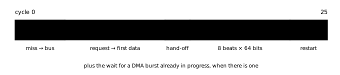
Only the eight beats are bandwidth. The rest is latency: the pipeline noticing the miss, the controller taking the request and the PSRAM’s command and wait, the hand-off, and the pipeline restarting. More bandwidth doesn’t shorten any of it. An experiment with a dual-ported cache showed that refilling straight into the cache’s RAM, skipping the bridge, saved only 0.7% on a Doom timedemo.
Where 664 MB/s goes
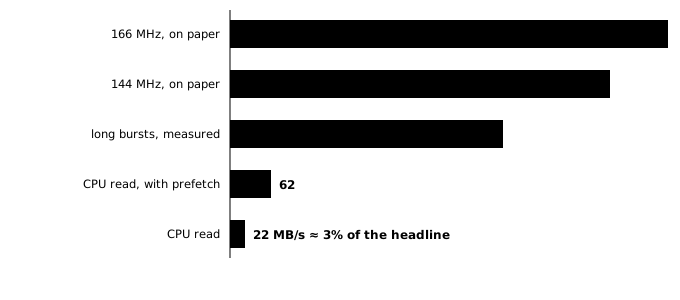
Run the bus at 144 MHz instead of 166, and it’s 576 MB/s. Pay the command and the latency on every burst, and long transfers measured 413 MB/s. But the CPU doesn’t make long transfers: it moves 64-byte lines, one at a time, and waits for each. A loop that does nothing but read memory gets 22 MB/s.
Prefetching (the Zicbop extension, part 2) lets a loop ask for the next line while it works on a current one, and the same loop reaches 62 MB/s. Writing gets help too: cbo.zero allocates a line in the cache as zeros without reading it from PSRAM, which makes memset and buffer fills faster. But a game doesn’t walk memory in a neat line. Most of its misses are unpredictable, and each one costs the full 25 cycles.
That’s the real budget of this machine, and much of the work in the game ports (part 6) is about missing less: a second cache way, data laid out so hot things don’t collide, and smaller working sets.
The bill
The controller and its PHY take about 310 logic cells, the bridge about 250, and neither uses block RAM: the line buffers are LUT RAM, and the transfer RAM (4 blocks) belongs to the video side. The I/O blocks are hard silicon: 24 OSER4s and 16 IDES4s.