m9b · part 1 of 6
A retro-style computer on a Tang Nano 9K
A 36 MHz RISC-V CPU with caches, 8 MB of RAM, 720x480@60Hz on HDMI with 48 kHz stereo sound, two USB ports and an SD card, all built from the 8,640 lookup tables of a $15 FPGA board. To put it through its paces, I ported Doom, Descent, Tyrian, System Shock and Ultima VII - and they all run pretty decently.
These posts will cover the system design: what went into the chip, where the logic cells went, how fast the various bits could go, and how the games were tuned to run on the result. This first part is the overview: the FPGA, the system around the CPU and its clocks. The following parts will take individual subsystems apart.
The Tang Nano family
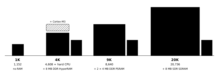
Sipeed’s Tang Nano boards put a Gowin FPGA on a board the size of a stick of gum, with a USB-C port for programming the FPGA and various other connectors depending on the model. The four boards span almost a factor of twenty in logic:
| Board | FPGA | LUT4 | Block RAM | RAM in package | Hard CPU |
|---|---|---|---|---|---|
| Tang Nano 1K | GW1NZ-1 | 1,152 | 8 KB | none | no |
| Tang Nano 4K | GW1NSR-4C | 4,608 | 20 KB | 8 MB HyperRAM | Cortex-M3 |
| Tang Nano 9K | GW1NR-9 | 8,640 | 52 KB | 8 MB PSRAM (2 dies) | no |
| Tang Nano 20K | GW2AR-18 | 20,736 | 92 KB | 8 MB SDRAM | no |
The 20K is where most retro-computing on Tang Nano boards happens: there’s quite a few cores out there. The 1K is enough for a small CPU, but not for a computer around it, and it lacks the HDMI connector of the other boards in the series. The 4K has a Cortex-M3 built into the silicon, which would be a great base for a small computer system, but the way its address bus is handled makes it tricky to use - I’ll likely write more about this one later.
The 9K has no hard CPU. If there’s going to be a processor, it has to be built from the same 8,640 cells as everything else. That’s the challenge I picked, with a few non-negotiables to start with:
- No extra processing. While it would be tempting to bind in the BL702 by reflashing it, that’s not going to happen here. It’s only the FPGA.
- A generic computer. The games are test cases, and I don’t want to design specific hardware accelerators for any one of them.
- Real input and output. HDMI with sound, USB keyboards and mice, an SD card with a real file system.
- Port the software, don’t rewrite it. Use the C/C++ source code that’s out there and port to the board. Some optimization is acceptable, but the game should look, sound and interact exactly like the original.
And that’s it. The baseline would be to just kick off LiteX and generate a baseline system, since it supports this board, but the performance of the result is sadly kind of terrible (at least at the time of writing).
Three dies in one package
The chip on the board, a GW1NR-LV9QN88P, is really three dies in one package: the FPGA itself, and two 32 Mbit PSRAMs (4 MB each). Each PSRAM has its own 8-bit, double-data-rate bus to the FPGA, rated up to 166 MHz. None of those wires leave the package; on the board, the chip looks like any other 88-pin FPGA.
Those numbers frame everything else. 52 KB of block RAM is less memory than a typical 1980s home computer had: a single VGA frame as used by our test games, is 320 × 200 bytes, and wouldn’t fit in all 26 blocks put together. So the programs and their data live in the PSRAM, and the block RAM goes to caches and buffers. The PSRAM’s 664 MB/s is a number on paper: part 3 follows it down to what the CPU actually gets, which is a small fraction.
There’s no dedicated hardware for anything else. The chip has serializers fast enough for HDMI and the RAM, but the encoder is logic. Sound travels inside the HDMI signal, so that’s logic too. The board has no USB host port; the USB sockets are wired straight to I/O pins, and the protocol is handled in logic too.
The system
Here is the whole computer, by clock domain.
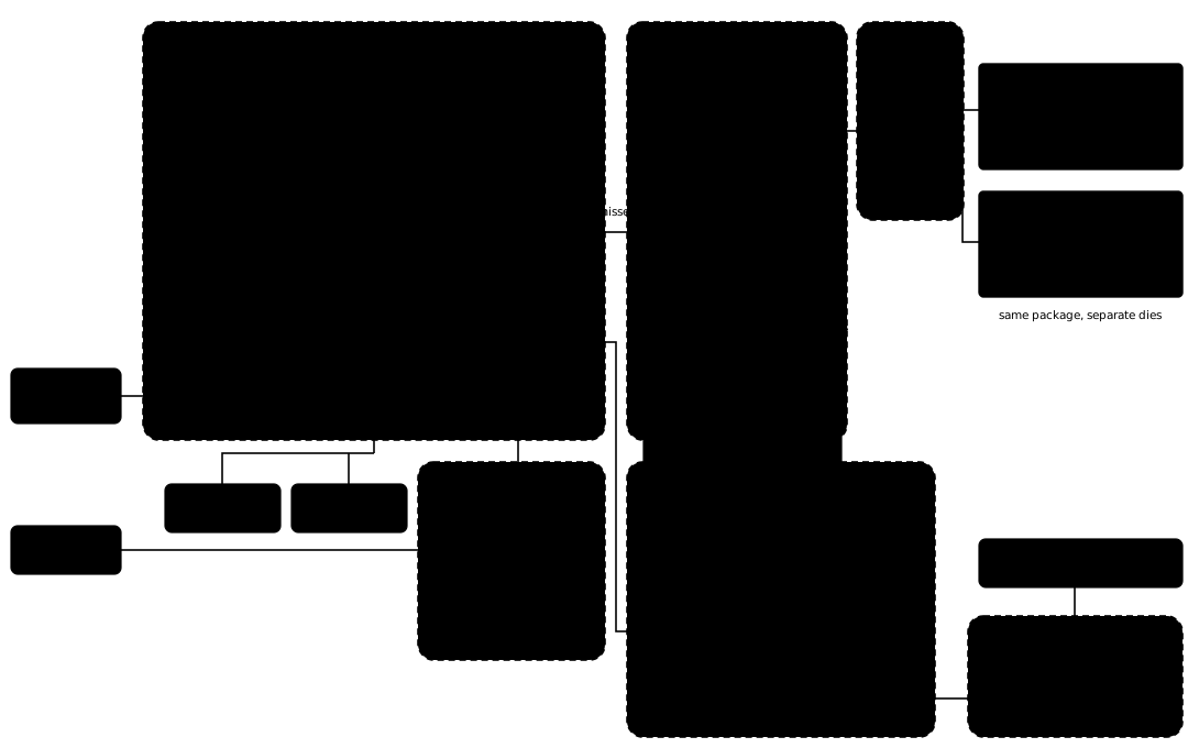
The top level design is fairly straghtforward. I picked a high performance RISC-V CPU core (vexiiRiscv) and used a good share of the block memory to provide it with ample cache (24 KB of our 52 KB), since the latency of the DDR RAM is pretty scary, and we really don’t want to have to hit it too often. Part 2 goes into a lot more detail on the CPU features and subsystem design. The DDR PSRAM controller accesses both dies in lockstep, generating a single command stream that is duplicated to both dies. The PHY is a simple collection of serializers and deserializers. Part 3 details the inner workings of the controller. The PSRAM controller is also connected to the graphics and audio engine via a transfer RAM, which buffers 2 scanlines of video data and 2 audio buffers. The video engine also has a dedicated RAM for the palette and line table, which can be written directly by the CPU to reduce latency. The HDMI encoder is a simple TMDS encoder that takes the pixel data and generates the HDMI signal. Part 4 looks at this subsystem. The USB host engine is a microcoded core that handles the USB protocol and provides a simple register interface to the CPU. Part 5 looks at this subsystem. The built-in peripherals are rounded out by a UART for debugging and an SPI interface for talking to the flash chip and SD card.
Clocks
All the clocks come from the board’s one 27 MHz crystal, through the chip’s two PLLs and three of its clock dividers. There are a few frequencies we have no control over and that must be respected in order for the system to work: one of these is the dot clock for a VESA standard display mode (in this case 27 MHz for the 720x480 display mode I chose), which also means we need a 5 * 27 = 135 MHz clock for driving the serializers. The other is the 12 MHz clock for USB, which is a standard frequency for full-speed USB. For everything else, we need to use divisors or multiples of these clocks, since we already need both PLLs since 12 and 27 are not integer multiples of each other. I ended up clocking everything off USB clock multiples, with 36 MHz, 72 MHz and 144 MHz clocks for the hardware. Keeping clocks well aligned is very important, since clock domain crossings cost latency.
| Clock | MHz | Made by | Why that number |
|---|---|---|---|
| TMDS bit clock | 135 | pll_hdmi: 27 × 5 | HDMI sends 10 bits per pixel per channel: 270 Mbit/s, on both edges of 135 MHz |
| Pixel clock | 27 | 135 ÷ 5 | 720 × 480 at 59.94 Hz is a 27 MHz mode. Divided from the bit clock so the serializers' two clocks are in phase by construction |
| PSRAM I/O | 144 | pll_main: 27 × 16 ÷ 3 | Rated 166 MHz; 144 is the fastest that also divides into 48 for USB |
| PSRAM controller | 72 | pll_main ÷ 2 | The I/O serializers take 4 bits per pin per controller cycle |
| CPU | 36 | 72 ÷ 2 | As fast as the CPU closes timing (37.8 MHz at the last build), and synchronous with the controller |
| USB | 12 | pll_main ÷ 3, then ÷ 4 | Low-speed USB is 1.5 Mbit/s, sampled 8 times per bit: exactly 12 MHz |
Where the cells go
After place and route, the design uses 7,560 of the 8,640 logic cells (88%) and 25 of the 26 block RAMs. The tighter limit is actually the slices: logic cells are packed in pairs, and 97% of those pairs are in use. At that fill level, the clock speed a build reaches depends heavily on where the tools happen to place things, and every build ends with a look at the timing report.
| Block | Logic cells | Block RAMs | What the block RAM holds |
|---|---|---|---|
| CPU (with its caches) | ≈ 4,340 | 18 | data L1: 8 data L1 tags: 2 fetch L1: 4 fetch L1 tags: 1 branch predictor: 1 registers: 2 |
| HDMI encoder | ≈ 630 | – | |
| Video engine, video RAM | ≈ 490 | 2 + 4 | palette and line table: 2 transfer RAM (line buffers, audio): 4 |
| PSRAM controller, bridge | ≈ 560 | – | the bridge’s line buffers are LUT RAM |
| USB host, two ports | ≈ 490 | 1 | the microcode ROM |
| UART, SPI, flash reader | ≈ 270 | – | |
| Glue: I/O decode, clock crossings, resets | ≈ 690 | – |
Per-block numbers come from synthesis and are approximate: place and route optimizes across blocks, and its total is the 7,560.
More than half the chip is the CPU. Everything else is about as compact as I could get it, and I sacrificed features that were not immediately useful along the way. For example, the first versions had a hardware text mode, and that got trimmed off (which also lef to a better looking proportional font on the startup screen). I also trimmed out all forms of audio synthesis, keeping only a simple wave audio out.
The rest of the series
- The CPU: why VexiiRiscv, and what every option costs and buys: the caches, the branch predictor, the extensions that fit and the ones that didn’t, 24-bit addresses, and a block RAM bug that shaped the data cache.
- The PSRAM controller: two dies driven as one 16-bit memory, the bridge to the CPU, and where 664 MB/s goes.
- HDMI: the encoder, a video engine built around a line table, and sound in the blanking periods.
- USB: a USB host from bare pins, one microcoded engine shared by two ports, and why two resistors matter.
- The games: porting five 1990s PC games to a machine slower than the PCs they were written for, and what each needed.
The source, the RTL and the game ports, is on GitHub: m9b-system ties together the SoC (m9b-core) and the game ports, each a repository of its own.
Credits
m9b stands on a lot of other people’s work. Each repository’s README lists exactly what it uses, at which version, and what was changed.
The hardware and its firmware:
- SpinalHDL/VexiiRiscv (Charles Papon): the CPU, built from a fork with m9b’s options
- hdl-util/hdmi (Sameer Puri): the HDMI encoder, with audio
- nand2mario/usb_hid_host (based on hi631’s work): the USB host
- FatFs (ChaN): the FAT file system on the SD card
- picolibc: the C library, and the programs’ linker script
- Wohlstand/libADLMIDI: the OPL3 emulation the music is rendered with, on the PC