<?xml version="1.0" encoding="utf-8"?><feed xmlns="http://www.w3.org/2005/Atom" ><generator uri="https://jekyllrb.com/" version="3.10.0">Jekyll</generator><link href="https://the-parts-bin.github.io/feed.xml" rel="self" type="application/atom+xml" /><link href="https://the-parts-bin.github.io/" rel="alternate" type="text/html" /><updated>2026-10-30T08:59:26+01:00</updated><id>https://the-parts-bin.github.io/feed.xml</id><title type="html">The Parts Bin</title><subtitle>Projects, builds and experiments from The Parts Bin.</subtitle><author><name>The Parts Bin</name></author><entry><title type="html">Re-retro: five games on 36 MHz</title><link href="https://the-parts-bin.github.io/m9b/games/" rel="alternate" type="text/html" title="Re-retro: five games on 36 MHz" /><published>2026-10-28T09:05:00+01:00</published><updated>2026-10-28T09:05:00+01:00</updated><id>https://the-parts-bin.github.io/m9b/m9b-6-games</id><content type="html" xml:base="https://the-parts-bin.github.io/m9b/games/"><![CDATA[<p class="lede">The five games were written for DOS PCs of the early 1990s. Their modern source ports assume a modern machine. Running them on m9b meant undoing some of that modernization: putting them back on a diet of memory, cycles and sound hardware that’s in some ways tighter than the PCs they first ran on.</p>

<div class="shorts wide"><figure class="short" data-yt="tZcOZ9u-YoA"><div class="frame"></div><figcaption>Doom</figcaption></figure><figure class="short" data-yt="jezV9N5zn6w"><div class="frame"></div><figcaption>Descent</figcaption></figure><figure class="short" data-yt="sWzJSCo9wvY"><div class="frame"></div><figcaption>Tyrian</figcaption></figure><figure class="short" data-yt="qfxQ3Utthho"><div class="frame"></div><figcaption>System Shock</figcaption></figure></div>

<div class="table-wrap wide">

  <table>
    <thead>
      <tr>
        <th>Game</th>
        <th>Port of</th>
        <th>Speed on m9b</th>
        <th>What mattered most</th>
      </tr>
    </thead>
    <tbody>
      <tr>
        <td><a href="https://github.com/the-parts-bin/m9b-doom">Doom</a> (1993, shareware)</td>
        <td><a href="https://github.com/ozkl/doomgeneric">doomgeneric</a></td>
        <td>≈ 22 fps (timedemo)</td>
        <td>the column and span drawers; the data cache</td>
      </tr>
      <tr>
        <td><a href="https://github.com/the-parts-bin/m9b-descent">Descent</a> (1995, shareware)</td>
        <td><a href="https://github.com/dxx-rebirth/dxx-rebirth">D1X Rebirth</a> 0.40</td>
        <td>≈ 10 fps, from 5</td>
        <td>the texture mapper’s divides; the cockpit</td>
      </tr>
      <tr>
        <td><a href="https://github.com/the-parts-bin/m9b-tyrian">Tyrian 2.1</a> (1995)</td>
        <td><a href="https://github.com/opentyrian/opentyrian">OpenTyrian</a></td>
        <td>35 fps, full speed, from 17</td>
        <td>one bounds check per pixel</td>
      </tr>
      <tr>
        <td><a href="https://github.com/the-parts-bin/m9b-sshock">System Shock</a> (1994)</td>
        <td><a href="https://github.com/Interrupt/systemshock">Shockolate</a></td>
        <td>≈ 7.4 fps, from 5.8</td>
        <td>memory: 17 MB cutscenes; misaligned reads; divides</td>
      </tr>
      <tr>
        <td><a href="https://github.com/the-parts-bin/m9b-exult">Ultima VII</a> (1992), both games</td>
        <td><a href="https://github.com/exult/exult">Exult</a> 1.12.1</td>
        <td>7–13 fps</td>
        <td>memory: a 6.2 MB heap in under 6 MB</td>
      </tr>
      <tr>
        <td><a href="https://github.com/the-parts-bin/m9b-u7">Ultima VII</a>, original engine</td>
        <td><a href="https://github.com/Kitrinx/Ultima7_Decomp">Ultima7_Decomp</a></td>
        <td>8–10 fps (the engine’s limit is 10)</td>
        <td>word-aligned heap blocks; sprites and tiles a word at a time</td>
      </tr>
    </tbody>
  </table>

</div>

<h2 id="the-machine-they-land-on">The machine they land on</h2>

<p>m9b is in-order, has no floating-point unit, and runs at 36 MHz with 8 MB of RAM behind caches whose misses cost about 25 cycles each (<a href="../psram/">part 3</a>). It has no sound chip and no MIDI synthesizer. It does have a 32-bit hardware multiplier and divider, a reasonably fast SD card, and a video engine that does page flipping and scaling for free.</p>

<p>The software is simply ported, not rewritten. Each game is its upstream source, trimmed to what the build needs, with every change marked, and a platform layer of its own in place of SDL.</p>

<h2 id="one-platform-for-five-games">One platform for five games</h2>

<p>All five share a <a href="https://github.com/the-parts-bin/m9b-core/tree/main/runtime">small runtime</a>, first written for Doom:</p>

<ul>
  <li><strong>C library and files:</strong> picolibc, with its system calls mapped onto the console UART and onto FatFs, so <code class="language-plaintext highlighter-rouge">open</code>, <code class="language-plaintext highlighter-rouge">read</code> and <code class="language-plaintext highlighter-rouge">lseek</code> work on the SD card. The C++ ports (System Shock’s physics, all of Exult) use picolibc’s libstdc++, exceptions included.</li>
  <li><strong>A trap handler</strong> that dispatches the interrupts, and emulates misaligned loads and stores: the CPU traps on them, and old game code is full of them.</li>
  <li><strong>Video:</strong> every game draws its 320 × 200, 8-bit screen as it always did. The port copies it to one of three display buffers, cleans it out of the data cache, and the vertical-blank interrupt points the line table at it, with each line doubled horizontally and shown on 2 or 3 screen lines: the 4:3 picture a VGA monitor gave (<a href="../hdmi/">part 4</a>).</li>
  <li><strong>Sound effects</strong> are mixed in the audio interrupt, at 12 or 24 kHz rather than 48, with each result held for 4 or 2 output samples. The effects are 11 or 22 kHz samples to begin with, so nothing is lost, and the mix costs a few percent of the CPU instead of a tenth.</li>
  <li><strong>Loading:</strong> programs live on the SD card, picked from a boot menu. The SD driver reads runs of sectors with one command, 32 bits at a time: Doom’s level load went from 4.6 s to 1.7 s as the SD card driver improved.</li>
</ul>

<h2 id="music-rendered-once-streamed-forever">Music: rendered once, streamed forever</h2>

<p>All five games composed their music for a synthesizer: an AdLib or Sound Blaster’s Yamaha OPL FM chip, or a Roland MT-32. None fits. An open-source OPL2 core needs 1,337 cells and 4 block RAMs on this chip, which has about a thousand cells and one block RAM to spare. A software synthesizer would cost 10 to 15% of the CPU before the game draws anything, and the ports’ own emulators compute in floating point.</p>

<p>So the music is rendered once, on a PC, and streamed from the SD card during play. For four of the games, that’s libADLMIDI’s emulation of the OPL3 chip playing each game’s own instruments and its sound driver’s volume rules: Doom’s GENMIDI bank, Descent’s HMI banks, System Shock’s AIL timbres; Tyrian through its own player and OPL emulator. Ultima VII uses Exult’s recordings of a real Roland MT-32, the synthesizer it was composed for. Every track comes out as 24 kHz mono WAV at a common loudness, streamed through a ring buffer in PSRAM that the main loop tops up and the audio interrupt drains.</p>

<p>The results aren’t small: 81 MB for Doom, 69 for Descent, 128 for Tyrian, 95 for System Shock, 208 for Ultima VII. SD cards are big so that’s not much of a problem.</p>

<p>System Shock needed one more step. Its music is adaptive: each theme is up to 54 short sequences, and a music AI starts them on up to 8 threads, a main piece and layers over it, choosing what comes next from what’s happening. Each sequence is rendered on its own (227 files), and the port implements the music driver’s interface on top of them: the game’s own AI still picks the pieces, the port streams up to eight of them at once and mixes them.</p>

<h2 id="doom-the-drawers">Doom: the drawers</h2>

<p>Doom spends its time in two loops: <code class="language-plaintext highlighter-rouge">R_DrawColumn</code>, which draws walls and sprites a vertical column at a time, and <code class="language-plaintext highlighter-rouge">R_DrawSpan</code>, which draws floors and ceilings a horizontal row at a time. Together they’re 40% of the frame.</p>

<div class="table-wrap">

  <table>
    <thead>
      <tr>
        <th>Change (CPU at 27 MHz at the time)</th>
        <th style="text-align: right">2,000 frames</th>
        <th style="text-align: right">fps</th>
      </tr>
    </thead>
    <tbody>
      <tr>
        <td>Baseline</td>
        <td style="text-align: right">181.0 s</td>
        <td style="text-align: right">11.0</td>
      </tr>
      <tr>
        <td>Column and span drawers: locals, 4 pixels per iteration</td>
        <td style="text-align: right">157.2 s</td>
        <td style="text-align: right">12.7</td>
      </tr>
      <tr>
        <td>Page flip in the vertical-blank interrupt</td>
        <td style="text-align: right">144.5 s</td>
        <td style="text-align: right">13.8</td>
      </tr>
      <tr>
        <td>Range checks off</td>
        <td style="text-align: right">141.3 s</td>
        <td style="text-align: right">14.2</td>
      </tr>
      <tr>
        <td>Drawing straight into the display buffers</td>
        <td style="text-align: right">138.0 s</td>
        <td style="text-align: right">14.5</td>
      </tr>
    </tbody>
  </table>

</div>

<p>From there, the hardware took over: the CPU going synchronous at 36 MHz, the 2-way data cache, faster SD reads, <code class="language-plaintext highlighter-rouge">cbo.zero</code> in <code class="language-plaintext highlighter-rouge">memset</code> and <code class="language-plaintext highlighter-rouge">memcpy</code>, the radix-4 divider. The timedemo now runs at about 22 fps. Before the second cache way, moving a buffer by a few hundred bytes changed Doom’s speed by 2%: a column of the screen touches 200 cache lines, and whatever else was hot fought it for them.</p>

<h2 id="descent-one-divide-in-sixteen">Descent: one divide in sixteen</h2>

<p>Descent is a true 3D game with perspective-correct texture mapping, and D1X’s C version of the texture mapper divides by depth for every pixel: 70 cycles or more each. At first, texture mapping was two thirds of the time and the game ran at 5 fps.</p>

<ul>
  <li><strong>The texture mapper</strong> now computes exact texture coordinates every 16 pixels, from one reciprocal, and steps linearly in between, with both coordinates packed into one word as Doom’s span drawer does, four pixels per iteration.</li>
  <li><strong>Divides</strong> that the original did in assembly, 64 by 32 bits, now take two hardware divides instead of a bit-by-bit loop.</li>
  <li><strong>The cockpit</strong> is a full-screen bitmap with a transparent hole for the 3D view, and D1X redrew it, with every gauge, every frame. Now its opaque runs are rendered once, it’s redrawn only where the 3D view can reach, and the texture mapper skips scanline pieces the cockpit will cover anyway. Cockpit and gauges went from 8% of the time to 1%.</li>
  <li><strong>Key polling</strong> checked all 256 keys on every query, 6% of the time; now only held keys are checked.</li>
</ul>

<p>About 10 fps in the first level, with the full cockpit.</p>

<h2 id="tyrian-one-check-per-pixel">Tyrian: one check per pixel</h2>

<p>Tyrian’s profile showed two thirds of the time in one function, drawing the three scrolling background layers a byte at a time, each pixel checked against the screen’s edges. Rows that are wholly on screen now skip the checks, and the game went from 17 to 35 fps: its full speed, set by its own timer, with time to spare. Its music needed rendering too: OpenTyrian’s OPL emulator computes envelopes in floating point for every sample.</p>

<h2 id="system-shock-back-to-1994s-memory">System Shock: back to 1994’s memory</h2>

<p>Shockolate is Night Dive’s 2018 release of the Macintosh source, made portable. The Mac version, and the port, assumed far more memory than 1994’s DOS version: starting level 1 took 5.3 MB of heap, and a cutscene 17 MB. m9b has 5.1 MB of heap for it.</p>

<ul>
  <li><strong>The resource table</strong> had an entry for each of 32,768 possible resource IDs: 1.1 MB. System Shock’s go up to about 5,500.</li>
  <li><strong>Compound resources</strong> (a texture’s sizes, a critter’s frames) were read whole when one item was needed, and the item decoded into a copy. Now only the index is read, and each item when first asked for.</li>
  <li><strong>Movies</strong> were loaded whole (14 MB for the intro), their sound unpacked into another 2.5 MB, and kept after playing. Now they stream from the file as they play, and use the low-resolution cutscenes the DOS version shipped, a quarter of the decoding.</li>
</ul>

<p>Level 1 now takes 2.8 MB, a cutscene about 0.2 MB. Speed came from two places: the texture unpacker read words at odd addresses, 97% of the misaligned accesses the trap handler was emulating, and the fixed-point divides went through a 64-bit software routine instead of the hardware divider. With those fixed and the radix-4 divider in the CPU, a saved game went from 5.8 to 7.4 fps. Double clicks needed their own fix: at 7 fps, two clicks fell between polls of the mouse, so the buttons are now sampled in the audio interrupt, with their times.</p>

<h2 id="ultima-vii-a-heap-diet">Ultima VII: a heap diet</h2>

<p>The original Ultima VII is 16-bit real-mode code on Origin’s own memory manager, with no source. Exult reimplements its engine in C++17, and plays the original data. Starting The Black Gate took 6.2 MB of heap; m9b has 5.8 MB to give it, and the C library’s allocator lost another 540 KB to holes, until Doug Lea’s malloc replaced it.</p>

<ul>
  <li><strong>Usecode</strong>, the games’ scripts, 1.5 MB of bytecode, was read whole at the start. Now each function is read when a call needs it, and the least recently used are dropped to keep 192 KB at most.</li>
  <li><strong>Shapes</strong> read from the 7.3 MB shape file stayed in memory forever. Now the least recently used are dropped past 384 KB.</li>
  <li><strong>Terrain</strong> took 4 KB per kind of map chunk, and Trinsic has 120; now 3 bytes per tile. Rendered floors are cached for 24 chunks instead of 100.</li>
</ul>

<p>Trinsic, a few minutes in, now peaks at 4.1 MB, with room for the MT-32 music and sound effects. It plays at 7 to 13 fps. Exult does more work per object than the 1992 engine did on a 386, and that’s the next thing to look at.</p>

<p>The 1992 engine itself runs too. <a href="https://github.com/Kitrinx/Ultima7_Decomp">Ultima7_Decomp</a> is a decompilation of both DOS games into portable C and C++, and <a href="https://github.com/the-parts-bin/m9b-u7">m9b-u7</a> gives it a platform layer for the board. The game gets the DOS memory it expected, in a 4 MB arena, and needed few changes: its far heap keeps blocks word-aligned, so the CPU doesn’t trap, and sprite spans and tiles are drawn a word at a time. Walking around Trinsic, it runs at 8 to 10 fps, against its own limit of 10 steps a second. Its music and sound effects are the same MT-32 recordings the Exult port uses.</p>

<h2 id="how-the-ports-were-tested">How the ports were tested</h2>

<ul>
  <li><strong>The Doom timedemo</strong> plays a fixed demo and checksums every frame, so every hardware and software change can be compared by its run time, with proof that it draws the same pictures.</li>
  <li><strong>Host test harnesses</strong> run System Shock and Ultima VII, with the same port code, on 32-bit x86 Linux, holding them to the board’s heap and filling new memory with garbage as the board would. Memory diets were done there, then checked on the board.</li>
  <li><strong>Remote control:</strong> a running game answers screenshot requests over the serial port and takes key presses from it, so a game can be driven and checked without watching the display for automated testing.</li>
  <li><strong>Profiling:</strong> a profile build samples the program counter from an interrupt and sends the histogram over the serial port.</li>
</ul>

<p>None of the five games is fast by today’s standards. But they run in full, with their music, in a chip whose hardware most likely was not designed for them.</p>]]></content><author><name>The Parts Bin</name></author><summary type="html"><![CDATA[Porting Doom, Descent, Tyrian, System Shock and Ultima VII to a 36 MHz RISC-V computer in a Tang Nano 9K: the shared platform, pre-rendered music, memory diets and the hot loops of each game.]]></summary></entry><entry><title type="html">Two USB ports, one engine</title><link href="https://the-parts-bin.github.io/m9b/usb/" rel="alternate" type="text/html" title="Two USB ports, one engine" /><published>2026-10-28T09:04:00+01:00</published><updated>2026-10-28T09:04:00+01:00</updated><id>https://the-parts-bin.github.io/m9b/m9b-5-usb</id><content type="html" xml:base="https://the-parts-bin.github.io/m9b/usb/"><![CDATA[<p class="lede">The board’s only USB port belongs to the programmer. To plug in a keyboard and a mouse, the FPGA has to be a USB host itself, with nothing but its own pins, and on a chip this full, two ports had to share one host.</p>

<h2 id="a-host-from-bare-pins">A host from bare pins</h2>

<p>The Tang Nano 9K’s USB-C port goes to a BL702 microcontroller that acts as the JTAG programmer and serial port. It’s a USB <em>device</em>, like a keyboard, and two devices can’t talk to each other.</p>

<p>A full USB host controller is a large piece of hardware. But keyboards, mice and gamepads can all fall back to the oldest and slowest mode: <strong>low speed</strong>, 1.5 Mbit/s, with a simple fixed report format called the <strong>boot protocol</strong>. At that speed, ordinary 3.3 V pins will do. Each USB-A socket’s D+ and D− go straight to two header pins, and power and ground come from the header too. And each data line gets a 15 kΩ resistor to ground, as the USB specification asks of a host. Remember those resistors.</p>

<h3 id="low-speed-usb-briefly">Low-speed USB, briefly</h3>

<ul>
  <li><strong>Attach:</strong> a low-speed device pulls D− up through 1.5 kΩ. That’s how the host knows something is plugged in, how fast it is, and, as it turned out, which wire is which.</li>
  <li><strong>Bits</strong> are sent as changes: a 0 flips the lines, a 1 leaves them alone, and after six 1s a 0 is stuffed in so the receiver always has edges to lock onto.</li>
  <li><strong>Packets</strong> start with a sync pattern and a packet ID, and end with both lines driven low for two bit times.</li>
  <li><strong>Keep-alive:</strong> once every millisecond the host sends a short pulse, or the device suspends after 3 ms.</li>
  <li><strong>Enumeration:</strong> the host resets the bus, asks the device what it is, gives it an address, picks its configuration and asks for the boot protocol. Then it polls: a keyboard answers with 8 bytes (modifier keys and up to six keys held), a mouse with its buttons and how far it has moved.</li>
</ul>

<h2 id="a-host-made-of-microcode">A host made of microcode</h2>

<p>Doing all that in plain logic would take a big state machine. nand2mario’s <a href="https://github.com/nand2mario/usb_hid_host">usb_hid_host</a> does something smarter: it’s a tiny processor with its own small instruction set, running a microcode program from a ROM. It runs at 12 MHz, eight clocks per bit on the wire; the microcode does the reset, the enumeration, the polling and the timing, and the logic around it only shifts bits in and out.</p>

<p>m9b started with one copy per port, then shrank them in three steps.</p>

<h3 id="one-rom">One ROM</h3>

<p>Two cores meant two copies of the microcode, each in its own block RAM. But a block RAM has two read ports, and the microcode never changes, so both cores read the same ROM, one port each: one block RAM instead of two, at a time when there were only a couple left.</p>

<h3 id="smaller-cores">Smaller cores</h3>

<ul>
  <li>The 1 ms frame timer moved out of the core and became one timer for both ports.</li>
  <li>The watchdog counts frames instead of 12 MHz cycles: 10 bits instead of 24.</li>
  <li>The microcode program counter is 10 bits instead of 14: the program is 536 four-bit instructions.</li>
  <li>Upstream decodes each report by device type into key, mouse and gamepad outputs. The core now just keeps the last report’s first six bytes as they came, and software decodes them.</li>
</ul>

<p>That saved about 90 logic cells and 165 registers for the two ports. A differential simulation against the previous core, with random device traffic, matched cycle for cycle except for the watchdog’s new timeout.</p>

<h3 id="one-engine-for-both-ports">One engine for both ports</h3>

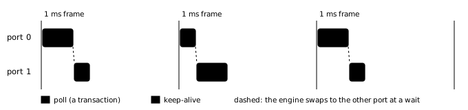
<p>The microcode spends most of its life waiting for the next 1 ms frame, and across that wait only a little state is live: its program counter, return address, one working register and a connected flag. So when the running port reaches a wait and the other port has a frame pending, the engine swaps that state with the other port’s saved copy and runs the other port. It’s a context switch, in hardware, between two microcode threads.</p>

<figure><img src="/assets/m9b/usb-shared-engine.svg" alt="One engine time-shared between two ports, frame by frame" /><figcaption>Schematic, not to scale. One port's poll delays the other's keep-alive by up to about 0.3 ms, well inside the 3 ms after which a device suspends.</figcaption></figure>

<p>Each port keeps what has to survive across frames: its own bus drive (a bus reset holds the lines low across several frames), its watchdog and its device type. The descriptor and report buffers are shared: descriptor fields are checked within one burst of transactions, and each port’s registers copy the report bytes within cycles of their arrival.</p>

<p>Sharing needed one new rule. Upstream’s core waits up to its watchdog (now 768 ms) for a device that doesn’t answer; with one engine, that would freeze the other port too. A new <strong>transaction timeout</strong>, 2,048 cycles (about 170 µs) from the start of a transaction, sends a silent port back to the start of its program. One engine instead of two saved another 136 logic cells and 150 registers. A simulation with two low-speed device models covers it: keyboard and mouse, a dead device on either port, nothing plugged in, unplug and replug.</p>

<h2 id="what-the-cpu-sees">What the CPU sees</h2>

<p>Each port is a handful of registers: the device type, a report counter, and the last report’s bytes. Mouse motion is also summed in hardware into a running position, so a game that looks once a frame loses none of the reports in between. Every report can raise an interrupt. The games compare each keyboard report with the previous one to make key presses and releases.</p>

<h2 id="fun-bugs">Fun bugs</h2>

<h3 id="it-was-the-connector">It was the connector</h3>

<p>Getting USB to work took many rounds, and the core was right the whole time. The USB ports are the only bit of hardware that was added to the Tang Nano 9k, and as with all things hand-soldered one of them obviously had a bad contact leading to a significant amount of wasted time.</p>

<p>What came out of it is a set of small diagnostic programs, loaded over the serial port: one shows which wire is pulled up and where the microcode spends its time, another records every change on the bus for 600 ms.</p>

<h3 id="the-keyboard-that-thought-it-was-ps2">The keyboard that thought it was PS/2</h3>

<p>My favourite keyboard happens to be a classic mechnical Cherry keyboard that is still manufactured, but hasn’t fundamentally changed over the decades. Unusually for a modern keyboard, it still comes with a passive PS/2 adapter in case you still happen to live in the 90s. It decides which at power-up by looking at the data lines: on a USB host, 15 kΩ pull-downs hold them low; on a PS/2 port, both are pulled high.</p>

<p>In the interest of saving hardware I’d left the 15k resistors out, relying on the FPGA’s internal pull-downs to do the job. But while the FPGA loads its configuration, its pins have weak pull-ups. So at power-up the keyboard saw both lines high, decided it was on a PS/2 port, and never spoke USB again until unplugged. It even broke flashing: with that keyboard on the pins, loading a new design failed its CRC check every time, which looked exactly like a broken bitstream.</p>

<p>The fix was to get a cheap modern keyboard, which you see in the videos.</p>

<h2 id="the-bill">The bill</h2>

<p>The two ports cost about 490 logic cells and one block RAM, for the shared microcode. With one ROM but two separate cores, before the other two steps, they took about 720.</p>]]></content><author><name>The Parts Bin</name></author><summary type="html"><![CDATA[A low-speed USB host for keyboards and mice from bare FPGA pins on the Tang Nano 9K: one microcoded engine shared by two ports.]]></summary></entry><entry><title type="html">Picture and sound over HDMI</title><link href="https://the-parts-bin.github.io/m9b/hdmi/" rel="alternate" type="text/html" title="Picture and sound over HDMI" /><published>2026-10-28T09:03:00+01:00</published><updated>2026-10-28T09:03:00+01:00</updated><id>https://the-parts-bin.github.io/m9b/m9b-4-hdmi</id><content type="html" xml:base="https://the-parts-bin.github.io/m9b/hdmi/"><![CDATA[<p class="lede">A 720 × 480 picture at 16 bits per pixel is 675 KB, thirteen times the chip’s block RAM. So the picture lives in PSRAM and is fetched a line at a time, just before it’s shown. The sound rides along in the same cable.</p>

<h2 id="the-signal">The signal</h2>

<p>The mode is 720 × 480 at 59.94 Hz, a standard TV mode with a 27 MHz pixel clock. Every frame is really 858 × 525 clocks: the visible picture, plus the horizontal and vertical blanking left over from CRTs. A line lasts 31.8 µs, and the signal never stops: whatever the CPU is doing, the next line has to be there.</p>

<p>HDMI sends each pixel on three channels, red, green and blue, each its own differential pair, plus a fourth pair for the clock. Each 8-bit colour becomes a 10-bit TMDS symbol, which keeps the line DC-balanced and cuts down on transitions. The encoder is based on <a href="https://github.com/hdl-util/hdmi">Sameer Puri’s open-source HDMI core</a>, one pixel per clock with a pipelined TMDS encoder. Its output goes to the chip’s hard OSER10 serializers, which shift ten bits out per pixel on both edges of the 135 MHz bit clock: 270 Mbit/s per channel.</p>

<p>The GW1NR-9 has no true LVDS outputs on these pins. Each differential pair is two ordinary 3.3 V pins driven in opposition (Gowin’s emulated LVDS buffer), which is fine at 270 Mbit/s.</p>

<h3 id="why-not-720p">Why not 720p</h3>

<p>The first design ran 1280 × 720, at 742.5 Mbit/s per channel. It worked as long as nothing else happened. As soon as the CPU got busy, on of my momitors lost sync, and another which is way more lenient on signal quality and encoding showed noise and blinked. I ruled things out one at a time: drive strength, PSRAM traffic, sudden load steps, the PLL’s reference clock, moving the CPU to another clock. None of them was it, and the severity changed from build to build with nothing but placement changing. Even the one build that looked fine only looked fine because its firmware was idle.</p>

<p>At 270 Mbit/s the link is solid on both monitors. It’s fewer pixels, but the games I wanted to get running initially only need 320 × 200 of them.</p>

<h2 id="the-video-engine">The video engine</h2>

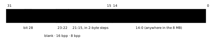
<p>Between the PSRAM and the encoder sits the video engine. Its central idea is a <strong>line table</strong>: one 32-bit entry per screen line, in a small video RAM, saying where that line’s pixels are in PSRAM and how to show them.</p>

<figure><img src="/assets/m9b/line-table-entry.svg" alt="A line table entry" /><figcaption>480 entries, one per visible line. Grey bits are unused.</figcaption></figure>

<p>Each visible line is one of three modes: <strong>16 bits per pixel</strong> RGB565 (1,440 bytes a line), <strong>8 bits per pixel</strong> through a 256-entry palette (720 bytes), or <strong>blank</strong>, which costs no memory bandwidth at all. An 8-bit line can also be <strong>doubled</strong>: each byte becomes two pixels inside a window, black outside it. The scroll field starts the line part-way into its first block.</p>

<p>Nothing says the lines have to come from one frame buffer, in order. Point two entries at the same data, and a line repeats; point them anywhere, and the screen splits, or parts of it scroll separately. The CPU can rewrite an entry at any time, and the change shows two lines later; the vertical-blank interrupt, at the start of line 480, is the natural moment to rewrite the whole table for the next frame. The hardware cost is one 32-bit read per line, and it replaces a stack of features a video chip would otherwise need: page flipping, scaling, split screens, scrolling.</p>

<h3 id="fetching-a-line">Fetching a line</h3>

<p>At the start of each line’s horizontal blanking, the engine reads the entry for the line after next and asks the PSRAM controller to DMA its pixels into one of two line buffers in the transfer RAM, an 8 KB dual-clock block RAM written at the controller’s 72 MHz and read at the pixel clock. While one buffer is on screen, the other fills. A 16-bit line is six 256-byte blocks (seven if the scroll offset makes it straddle one more), an 8-bit line three. The controller fits those bursts between the CPU’s cache misses (<a href="../psram/">part 3</a>), and the line is ready long before it’s needed.</p>

<h3 id="320--200-at-43">320 × 200 at 4:3</h3>

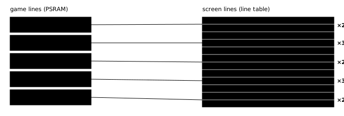
<p>All five games draw a 320 × 200 picture, a byte per pixel, the way a DOS PC’s VGA did. On a 4:3 monitor that mode had pixels 1.2 times taller than wide, and the games’ art was drawn for it. The line table recreates that for free:</p>

<figure><img src="/assets/m9b/line-doubling.svg" alt="Five game lines become twelve screen lines" /><figcaption>200 lines fill 480 at 2.4 screen lines each: 2, 3, 2, 3, 2, repeating. Horizontally, the doubled 8-bit mode turns 320 pixels into 640, centred in the 720.</figcaption></figure>

<p>The games triple-buffer the same way: each draws into one of three buffers, and the vertical-blank interrupt points the table at the finished one, so the picture never tears. The palette lives next to the table, so palette effects, such as Doom’s red damage flash, are free too.</p>

<h3 id="the-text-mode-that-went-away">The text mode that went away</h3>

<p>The engine once had a fourth mode: 90-column text, with a font in video RAM. Drawing text in software into an 8-bit line is fast enough for a boot screen, and it can use a proportional font. Removing the text mode freed about 250 cells and a block RAM, at a point where both were scarce.</p>

<h2 id="sound-in-the-blanking">Sound in the blanking</h2>

<p>The board has no audio jack, and adding a DAC would break the only-this-chip rule. But HDMI carries sound, and every display with speakers plays it.</p>

<p>HDMI is DVI with extras. In the blanking periods, where DVI sends nothing, HDMI can send packets, called <em>data islands</em>, in a different encoding (TERC4: 4 bits per 10-bit symbol), fenced by guard bands so the receiver can tell them from pixels. Three packet types matter for sound:</p>

<ul>
  <li><strong>Audio samples</strong>, here 48 kHz, 16-bit stereo. At 48 kHz there are about one and a half stereo samples per line, with plenty of blanking to carry them.</li>
  <li><strong>Audio clock regeneration</strong>, which tells the receiver how the sample rate relates to the pixel clock: for 27 MHz and 48 kHz, the standard pair N = 6144, CTS = 27000.</li>
  <li><strong>The audio infoframe</strong>, which describes the format.</li>
</ul>

<p>Sameer Puri’s core does all of this as well; the packet side is about 215 of its 630 cells.</p>

<h3 id="feeding-it">Feeding it</h3>

<p>The samples come from PSRAM, through the transfer RAM, like the pixels. There are two 1 KB halves, each 256 stereo samples, 5.33 ms of sound. The engine plays half A, then B, then A again, and each time it moves on it raises an interrupt: the half it just finished is free. The CPU writes the next 256 samples into PSRAM, cleans them out of its data cache so the PSRAM really has them, and writes that half’s pointer register, which DMAs them across. The delay from a game to the speaker is 5 to 11 ms.</p>

<p>The audio interrupt is also where the games mix their sound, and it taught the project’s sharpest lesson about this memory system. Doom’s first mixer produced all 48,000 output samples per second for every channel and cost 8 to 9% of the CPU. A version that summed into a 2 KB buffer first cost 12% of the whole game, not because of the arithmetic, but because that buffer, touched from an interrupt, kept evicting the game’s own data from the cache. Mixing at 12 kHz, close to the effects’ own 11 kHz, and holding each result for four output samples brought it down to between 1 and 4%. The later ports mix at 12 or 24 kHz the same way. Music is a different story, for <a href="../games/">part 6</a>.</p>

<p>The first sound the board makes, every time it starts, is a two-note chime, computed 256 samples at a time.</p>

<h2 id="the-bill">The bill</h2>

<div class="table-wrap">

  <table>
    <thead>
      <tr>
        <th>Block</th>
        <th style="text-align: right">Logic cells</th>
        <th style="text-align: right">Block RAMs</th>
      </tr>
    </thead>
    <tbody>
      <tr>
        <td>HDMI encoder: TMDS, timing</td>
        <td style="text-align: right">≈ 415</td>
        <td style="text-align: right">–</td>
      </tr>
      <tr>
        <td>HDMI encoder: data islands (audio)</td>
        <td style="text-align: right">≈ 215</td>
        <td style="text-align: right">–</td>
      </tr>
      <tr>
        <td>Video engine and video RAM</td>
        <td style="text-align: right">≈ 490</td>
        <td style="text-align: right">2</td>
      </tr>
      <tr>
        <td>Transfer RAM: line buffers and audio halves</td>
        <td style="text-align: right">–</td>
        <td style="text-align: right">4</td>
      </tr>
    </tbody>
  </table>

  <p class="table-caption">Synthesis estimates. The serializers, the PLL and the clock divider are hard silicon.</p>

</div>]]></content><author><name>The Parts Bin</name></author><summary type="html"><![CDATA[720x480 HDMI with 48 kHz audio from a Tang Nano 9K: the TMDS encoder, a video engine built around a per-line table, and sound in the data islands.]]></summary></entry><entry><title type="html">Two PSRAM dies, one memory</title><link href="https://the-parts-bin.github.io/m9b/psram/" rel="alternate" type="text/html" title="Two PSRAM dies, one memory" /><published>2026-10-28T09:02:00+01:00</published><updated>2026-10-28T09:02:00+01:00</updated><id>https://the-parts-bin.github.io/m9b/m9b-3-psram</id><content type="html" xml:base="https://the-parts-bin.github.io/m9b/psram/"><![CDATA[<p class="lede">Everything the CPU runs, and every pixel and sample the display gets, comes out of the two PSRAM dies in the package. On paper they deliver 664 MB/s. The CPU gets a few percent of that, and this part is about why, and what that means for the design.</p>

<h2 id="the-bus">The bus</h2>

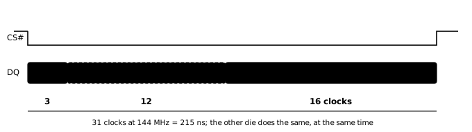
<p>Each of the two 32 Mbit dies has a HyperBus-style interface: eight data lines (DQ) used on both clock edges, a differential clock, a chip select, and a strobe called RWDS. A transfer goes like this:</p>

<ol>
  <li><strong>Command:</strong> six bytes that say read or write, and where. On a double-data-rate bus that’s three clocks.</li>
  <li><strong>Latency:</strong> the die makes you wait. m9b configures it for a fixed latency of 6 clocks, doubled: 12 clocks of nothing.</li>
  <li><strong>Data:</strong> a byte on every clock edge, for as long as chip select stays low.</li>
</ol>

<figure><img src="/assets/m9b/psram-read.svg" alt="A cache-line read on one die: 3 clocks of command, 12 of latency, 16 of data" /><figcaption>A 64-byte cache line is 32 bytes from each die. The command and the latency take half the time whatever the size of the transfer.</figcaption></figure>

<p>So a transfer has a fixed cost up front, and after that it’s cheap. Fetch one word, and you pay the whole setup for four bytes. Fetch a 64-byte line, and the setup is shared across all of it. That’s why the CPU’s caches move whole lines, and why the video engine fetches in 256-byte blocks.</p>

<p>The dies have no linear burst mode, only bursts that wrap within a configured length. m9b sets 128 bytes per die (configuration register CR0 = <code class="language-plaintext highlighter-rouge">0x8f1c</code>, written about 200 µs after reset). A cache line, 32 bytes per die and aligned, never reaches the wrap, and the controller ends it early by raising chip select. A DMA block is exactly one full wrap: 128 bytes per die, 256 in all.</p>

<h2 id="two-dies-in-lockstep">Two dies in lockstep</h2>

<p>The controller drives both dies with the same command, address and timing, each on its own data bus. Every 72 MHz controller cycle moves 32 bits per die, 64 bits in all: even 32-bit words live in die 0, odd ones in die 1. To everything else in the system, that’s one 8 MB memory with a 16-bit double-data-rate bus.</p>

<p>That’s where the headline number comes from: 166 MHz × 2 edges × 2 dies = 664 MB/s at the dies’ rated clock. m9b runs them at 144 MHz, so 576 MB/s.</p>

<h2 id="the-phy">The PHY</h2>

<p>The FPGA fabric can’t toggle pins at 144 MHz double data rate from plain logic. Each PSRAM pin goes through the chip’s hard I/O blocks instead: an OSER4 serializer takes four bits from the controller per 72 MHz cycle and shifts them out on both edges of the 144 MHz clock; an IDES4 deserializer does the reverse for reads.</p>

<p>Reads are the hard direction. The data comes back aligned to the die’s own view of the clock, after delays through the package and the pins, and the FPGA has to sample each bit in the middle of its window. Both the outgoing clock and the incoming data go through programmable delay lines (IODELAY). I swept the two delays in simulation and on the board, and picked the middle of the window that worked when the board was initially brought up at 148.5 MHz (that was an early version of the video hardware that still tried to do 720p, which has a dot clock of 74.25MHz, so the RAM was running at twice that). That delay also worked at 162 MHz, and at today’s 144 MHz. The read stream arrives skewed by one byte, and the controller reassembles each 32-bit word from two consecutive cycles. On typical RAM controllers, this delay is continuously calibrated and adjusted, which costs a lot of logic - using a fixed precalibrated delay is the secret to keeping the controller small. I tested on multiple boards in various conditions to convince myself it is reasonably stable.</p>

<p>The other trick is using the same controller across both dies, although there is a hefty price to pay for that: the two dies are independent, and may thus refresh at different times. The only way to not have to account for refreshes is to choose the fixed latency mode, which costs an extra 6 cycles on every access where no refresh is happening (which would be most of them).</p>

<h2 id="who-gets-the-bus">Who gets the bus</h2>

<p>Two kinds of client share the controller:</p>

<ul>
  <li><strong>Cache lines</strong>, from the CPU: a refill (read a 64-byte line) or a write-back (write a dirty one). The CPU is stalled on them, so they go first.</li>
  <li><strong>DMA</strong>, from the video engine: a video line (up to 1,440 bytes) or an audio block (1 KB) copied into the transfer RAM, the on-chip buffer the video side reads from. These come in 256-byte bursts.</li>
</ul>

<p>A cache line request goes ahead of any waiting DMA burst, but once a burst has started, it finishes. So a miss can land behind one, and that is part of its cost. The video side can afford to wait: it asks for each line two lines ahead of time (<a href="../hdmi/">part 4</a>).</p>

<p>The video load is modest. A full 720 × 480 picture at 16 bits per pixel is 41 MB/s; at 8 bits, 21 MB/s. The games use 8-bit lines, and sound adds less than 0.2 MB/s.</p>

<h2 id="the-bridge">The bridge</h2>

<p>Between the CPU’s caches and the controller sits the bridge: two 64-byte line buffers, one for refills and one for write-backs, in LUT RAM. The CPU side runs at 36 MHz, the controller side at 72.</p>

<ul>
  <li><strong>Refill first.</strong> When a miss evicts a dirty line, the cache wants to write it back and read the new one. The bridge takes the dirty line into its write buffer, but asks the controller for the refill first, since that’s what the CPU is waiting for; the write-back goes out afterwards.</li>
  <li><strong>Early start.</strong> The bridge hands the first 64-bit beat to the cache in the same cycle it arrives from the controller, and the rest as they come. That was worth about 5% on Doom.</li>
  <li><strong>One flop each way.</strong> Because the CPU’s clock is the controller’s divided by two (<a href="../">part 1</a>), the request and acknowledge cross between them with one flop each, instead of a two-flop synchronizer per direction.</li>
</ul>

<h2 id="anatomy-of-a-miss">Anatomy of a miss</h2>

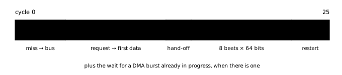
<p>Simulation shows where a clean data-cache miss spends its time, in CPU cycles at 36 MHz:</p>

<figure><img src="/assets/m9b/cache-miss.svg" alt="A data cache miss: 25 CPU cycles" /><figcaption>About 25 CPU cycles per miss. In that time the CPU could have run 25 instructions: miss once every 25 instructions, and it runs at half speed.</figcaption></figure>

<p>Only the eight beats are bandwidth. The rest is latency: the pipeline noticing the miss, the controller taking the request and the PSRAM’s command and wait, the hand-off, and the pipeline restarting. More bandwidth doesn’t shorten any of it. An experiment with a dual-ported cache showed that refilling straight into the cache’s RAM, skipping the bridge, saved only 0.7% on a Doom timedemo.</p>

<h2 id="where-664-mbs-goes">Where 664 MB/s goes</h2>

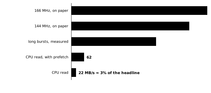
<figure><img src="/assets/m9b/psram-bandwidth.svg" alt="Bandwidth from the datasheet to the CPU" /><figcaption>The CPU rows are the boot firmware's benchmark: a loop that reads and sums memory, a line at a time, with and without a prefetch instruction for the next line.</figcaption></figure>

<p>Run the bus at 144 MHz instead of 166, and it’s 576 MB/s. Pay the command and the latency on every burst, and long transfers measured 413 MB/s. But the CPU doesn’t make long transfers: it moves 64-byte lines, one at a time, and waits for each. A loop that does nothing but read memory gets 22 MB/s.</p>

<p>Prefetching (the Zicbop extension, <a href="../cpu/">part 2</a>) lets a loop ask for the next line while it works on a current one, and the same loop reaches 62 MB/s. Writing gets help too: <code class="language-plaintext highlighter-rouge">cbo.zero</code> allocates a line in the cache as zeros without reading it from PSRAM, which makes <code class="language-plaintext highlighter-rouge">memset</code> and buffer fills faster. But a game doesn’t walk memory in a neat line. Most of its misses are unpredictable, and each one costs the full 25 cycles.</p>

<p>That’s the real budget of this machine, and much of the work in the game ports (<a href="../games/">part 6</a>) is about missing less: a second cache way, data laid out so hot things don’t collide, and smaller working sets.</p>

<h2 id="the-bill">The bill</h2>

<p>The controller and its PHY take about 310 logic cells, the bridge about 250, and neither uses block RAM: the line buffers are LUT RAM, and the transfer RAM (4 blocks) belongs to the video side. The I/O blocks are hard silicon: 24 OSER4s and 16 IDES4s.</p>]]></content><author><name>The Parts Bin</name></author><summary type="html"><![CDATA[Driving the Tang Nano 9K's two in-package PSRAM dies as one memory: the bus, the PHY, the bridge to the CPU's caches, and where 664 MB/s goes.]]></summary></entry><entry><title type="html">The CPU: VexiiRiscv, cut to fit</title><link href="https://the-parts-bin.github.io/m9b/cpu/" rel="alternate" type="text/html" title="The CPU: VexiiRiscv, cut to fit" /><published>2026-10-28T09:01:00+01:00</published><updated>2026-10-28T09:01:00+01:00</updated><id>https://the-parts-bin.github.io/m9b/m9b-2-cpu</id><content type="html" xml:base="https://the-parts-bin.github.io/m9b/cpu/"><![CDATA[<p class="lede">The CPU takes more than half of the chip: about 4,300 of its 8,640 logic cells and 18 of its 26 block RAMs. This part is about how it got there, and about what each of those cells and blocks buys.</p>

<h2 id="risc-v-the-obvious-choice">RISC-V: The obvious choice</h2>

<p>There’s quite a few open cores available out there, but for a project like this I wanted something that would work mostly out of the box: a well established toolchain and flexible but efficient verilog implementation were a must.</p>

<p>Considering the limited number of LUTs on this FPGA, RISC-V was the only serious contender here, since it provides a great developer experience for C or C++ program as well as a very extensible instruction set. The base set, RV32I, is about forty instructions; the M extension adds multiply and divide, which games use a lot, and then many others on top of that.</p>

<p>Any RISC-V core needs 32 registers of 32 bits. That’s 1,024 bits, a sixth of the chip’s 6,480 flip-flops if built from them, so in every core that fits here the register file is two block RAMs. Beyond that, the decisive factor is memory. Programs and data live in PSRAM, which takes dozens of CPU cycles to start a transfer. A core without caches would wait that long for every instruction.</p>

<h2 id="from-femtorv-to-vexiiriscv">From FemtoRV to VexiiRiscv</h2>

<p>The first version of the design ran FemtoRV32, from Bruno Levy’s <a href="https://github.com/BrunoLevy/learn-fpga">learn-fpga</a>, which is small and easy to read. The PetitBateau variant, with its floating-point unit, didn’t make 27 MHz: its slowest path compared two registers, decided a branch and computed the next address in one cycle, and on this chip that took longer than 37 ns. The Electron variant (RV32IM, no floating point) did make it, and it ran the first PSRAM tests. But FemtoRV has no caches.</p>

<p>Next came the default VexRiscv from LiteX: a five-stage pipeline with 4 KB instruction and data caches. This was quite a bit faster. Soon after came its successor, Charles Papon’s <a href="https://github.com/SpinalHDL/VexiiRiscv">VexiiRiscv</a>, for one reason above all: its data cache is <em>write-back</em>. VexRiscv’s writes every store through to memory; VexiiRiscv’s keeps stores in the cache until the line is evicted, so the PSRAM only ever sees whole 64-byte lines. That suits a memory that is slow to start a transfer and fast once it’s going.</p>

<p>VexiiRiscv isn’t a file you download, it’s a generator: you describe the core you want on the command line, and it writes out Verilog. Every option trades logic cells, block RAM and clock speed against performance, and the rest of this part is about those trades. This is the command line for the core in m9b, generated from <a href="https://github.com/the-parts-bin/m9b-VexiiRiscv/tree/m9b">a fork</a> with a few options of its own:</p>

<div class="language-plaintext wide highlighter-rouge"><div class="highlight"><pre class="highlight"><code>--xlen 32 --physical-width 24 --with-rvm --with-rvZcbm --with-rvZba
--lsu-software-prefetch --with-rvZicboz --div-radix 4
--with-btb --btb-hash-width 11 --btb-target-width 21 --with-ras
--relaxed-branch --relaxed-shift --regfile-async --allow-bypass-from 0
--fetch-l1 --fetch-wishbone --fetch-l1-sets 128 --fetch-l1-ways 1
--fetch-l1-mem-data-width-min 64
--lsu-l1 --lsu-l1-wishbone --lsu-wishbone --lsu-l1-sets 128 --lsu-l1-ways 2
--lsu-l1-mem-data-width-min 64 --lsu-l1-word-writes --lsu-l1-wishbone-unbuffered
--reset-vector 0
--region base=0,size=20000,main=1,exe=1          # user flash: cached
--region base=800000,size=800000,main=1,exe=1    # PSRAM: cached
--region base=400000,size=400000,main=0,exe=0    # I/O: uncached
</code></pre></div></div>

<h2 id="the-caches">The caches</h2>

<p>Both caches use 64-byte lines and talk to memory over 64-bit buses, a whole line per request. Long lines suit the PSRAM, whose fixed setup cost per transfer is shared across more bytes.</p>

<ul>
  <li><strong>Fetch L1: 8 KB, direct-mapped</strong> (128 sets of one line). 4 block RAMs for the data, 1 for the tags. Code mostly runs in loops, and going from 4 to 8 KB was worth about 2% on Doom.</li>
  <li><strong>Data L1: 16 KB, 2-way set-associative, write-back</strong> (128 sets of two lines). 8 block RAMs for the data, 2 for the tags.</li>
</ul>

<p>The data L1 was direct-mapped for most of the project: 256 sets of one line, every address with exactly one place to go. Its weakness is conflicts. Doom’s column drawer, for example, walks down a column of the screen, touching 200 different lines; whatever else is hot (the textures, the colour maps) lands on some of the same sets, and they evict each other. Moving a buffer by a few hundred bytes changed the timedemo by 2%. A second way removes most of that: on the Doom timedemo it was worth 14%.</p>

<p>This took a long time to land because of the block RAMs’ byte enables.</p>

<h3 id="the-byte-enable-bug">The byte-enable bug</h3>

<p>A cache that takes byte stores needs byte enables on its memory: a write mask that says which bytes of a word to change. Gowin’s block RAMs have them in practice, although they disappeared from the documentation a long time ago. And now I also know why: they don’t work reliably.</p>

<p>The first symptom was data corrupted by byte stores while the memory tests, which wrote whole words, kept passing. The simulation model was fine, timing was fine, the netlist was fine. A test design that exercises all 26 block RAMs eventually found the rule: <strong>when a port writes in two consecutive cycles, a byte lane that was enabled in the first write and disabled in the second gets written anyway</strong>, in 10 to 36% of cases, on every block, at 27, 36 and 72 MHz. An idle cycle or a read in between avoids it, and full-word writes never fail.</p>

<p>The first fix was to avoid byte enables altogether: one block RAM per byte lane, eight 2 KB lanes, which makes exactly 16 KB of direct-mapped cache. A 2-way cache of that shape would have needed 16 blocks.</p>

<p>The fix that made 2 ways possible is an option added in the fork, <code class="language-plaintext highlighter-rouge">--lsu-l1-word-writes</code>: the data L1 never writes partial words. A byte or half-word store reads its whole 32-bit word (through the pipeline’s bypass, so stores still in flight are included), merges its bytes in, and writes the word back. Each way’s bank then needs a write mask per 32-bit word, not per byte, and Gowin builds it from plain write enables: two blocks per way and word half, 8 blocks for 16 KB, the same as before. The boot firmware still checks byte, half-word and word stores in every lane, every time the board starts.</p>

<h2 id="what-each-option-is-worth">What each option is worth</h2>

<p>Every change was measured on the board, mostly with the Doom timedemo (a fixed demo, drawn one frame per game tic, so runs are comparable to the frame: they checksum every frame), and kept only if it paid for its cells.</p>

<div class="table-wrap">

  <table>
    <thead>
      <tr>
        <th>Option</th>
        <th style="text-align: right">Cost</th>
        <th style="text-align: right">Effect</th>
        <th>Kept?</th>
      </tr>
    </thead>
    <tbody>
      <tr>
        <td>Branch target buffer + return stack</td>
        <td style="text-align: right">1 block RAM + logic</td>
        <td style="text-align: right">Doom 13.5% slower without</td>
        <td>yes</td>
      </tr>
      <tr>
        <td>Zba (shift-and-add address instructions)</td>
        <td style="text-align: right">+141 cells</td>
        <td style="text-align: right">Doom 2.3% faster</td>
        <td>yes</td>
      </tr>
      <tr>
        <td>Zbb (bit manipulation, min/max)</td>
        <td style="text-align: right">+566 cells</td>
        <td style="text-align: right">CPU at 32–33 MHz</td>
        <td>no: doesn’t fit</td>
      </tr>
      <tr>
        <td>Zicbop (prefetch instructions)</td>
        <td style="text-align: right">+49 cells</td>
        <td style="text-align: right">read loop 22 → 62 MB/s</td>
        <td>yes</td>
      </tr>
      <tr>
        <td>Zicboz (<code class="language-plaintext highlighter-rouge">cbo.zero</code>: allocate a line without reading it)</td>
        <td style="text-align: right">small</td>
        <td style="text-align: right">fill loop 36 → 48 MB/s</td>
        <td>yes</td>
      </tr>
      <tr>
        <td>Second data L1 way (with word writes)</td>
        <td style="text-align: right">same block RAMs</td>
        <td style="text-align: right">Doom 14% faster</td>
        <td>yes</td>
      </tr>
      <tr>
        <td>Radix-4 divider (2 quotient bits per cycle)</td>
        <td style="text-align: right">+164 cells</td>
        <td style="text-align: right">System Shock 8%, Doom 1.2%</td>
        <td>yes</td>
      </tr>
      <tr>
        <td>Unbuffered data L1 bus (a miss one cycle shorter)</td>
        <td style="text-align: right">timing margin</td>
        <td style="text-align: right">Doom 0.6%</td>
        <td>yes</td>
      </tr>
      <tr>
        <td>Branches resolved a stage earlier</td>
        <td style="text-align: right">timing</td>
        <td style="text-align: right">Doom 1.0%</td>
        <td>no: misses 36 MHz</td>
      </tr>
    </tbody>
  </table>

  <p class="table-caption">Doom figures are timedemo run times; the MB/s are the boot firmware’s PSRAM benchmarks.</p>

</div>

<p>A few of these taught something beyond their number.</p>

<p><strong>The radix-4 divider</strong> looks like a luxury on a chip this full, but System Shock’s texture mapper divides once per span, about 150,000 times in five seconds of play. Halving the divide time made the whole game 8% faster.</p>

<p><strong>Prefetching</strong> helps loops that know where they are going: a read loop that prefetches the next line nearly triples its speed. Doom’s column drawer, which could in principle prefetch, gained at best 0.5%: most of its misses are the ones nobody can predict.</p>

<h2 id="smaller-and-faster-24-bit-addresses">Smaller and faster: 24-bit addresses</h2>

<p>The memory map needs 16 MB: flash at 0, I/O at 4 MB, PSRAM at 8 MB. A 32-bit CPU without an MMU still carries 32-bit addresses everywhere: in every copy of the program counter down the pipeline, in the branch and PC adders, in the load/store unit’s address stages, and in the cache tags.</p>

<p>VexiiRiscv’s <code class="language-plaintext highlighter-rouge">--physical-width</code> sets that width. At 24 bits, the tags shrink from 19 to 11 bits, every PC copy loses a byte, and anything at or above 16 MB traps. It saved 258 logic cells and 190 registers, and the CPU’s maximum clock went from 36.05 to 39.96 MHz: the critical path, from the branch predictor’s read to the PC increment, runs through the PC adder. Software only had to move to the new memory map.</p>

<p>A similar trick shrank the branch target buffer: with an 11-bit hash and 21 target bits, an entry is 36 bits, one block RAM instead of two.</p>

<h2 id="timing-at-88">Timing at 88%</h2>

<p>The CPU runs at 36 MHz, half the PSRAM controller’s clock. It has to stay synchronous with the controller (<a href="../">part 1</a>), so the next step up would be the full 72 MHz, which is out of reach. Every change has to keep the CPU above 36 MHz on a chip that is 88% full, and where things land matters more and more as it fills.</p>

<ul>
  <li><code class="language-plaintext highlighter-rouge">--relaxed-branch</code> was needed to reach 27 MHz at all, and <code class="language-plaintext highlighter-rouge">--relaxed-shift</code> (the shifter’s result is forwarded a stage later) to reach 36.</li>
  <li><code class="language-plaintext highlighter-rouge">--relaxed-btb</code> would shorten the branch predictor’s path, but didn’t route: it made a congestion hot spot.</li>
  <li>The place-and-route options decide between passing and failing: one routing option gave 35.7 MHz, another 38.75 for the same design. Every build ends with a look at the timing report.</li>
</ul>

<p>The last build reached 37.8 MHz, with 4% margin.</p>

<h2 id="the-bill">The bill</h2>

<div class="table-wrap">
<table>
  <thead><tr><th>Part of the CPU</th><th class="n">Block RAMs</th></tr></thead>
  <tbody>
    <tr><td>Data L1: data (2 ways × 2 word halves × 2 blocks)</td><td class="n">8</td></tr>
    <tr><td>Data L1: tags</td><td class="n">2</td></tr>
    <tr><td>Fetch L1: data</td><td class="n">4</td></tr>
    <tr><td>Fetch L1: tags</td><td class="n">1</td></tr>
    <tr><td>Branch target buffer</td><td class="n">1</td></tr>
    <tr><td>Register file</td><td class="n">2</td></tr>
    <tr class="hl"><td>Total, of the chip's 26</td><td class="n">18</td></tr>
  </tbody>
</table>
</div>

<p>Plus about 4,300 logic cells and two of the chip’s hard multiplier blocks. The Doom timedemo now runs at about 22 frames per second; the options above account for a good part of that, and the memory system in the next part for much of the rest.</p>]]></content><author><name>The Parts Bin</name></author><summary type="html"><![CDATA[How a VexiiRiscv RISC-V core was configured to fit a Tang Nano 9K: caches, branch prediction, extensions that fit and didn't, 24-bit addresses, and a block RAM bug.]]></summary></entry><entry><title type="html">A retro-style computer on a Tang Nano 9K</title><link href="https://the-parts-bin.github.io/m9b/" rel="alternate" type="text/html" title="A retro-style computer on a Tang Nano 9K" /><published>2026-10-28T09:00:00+01:00</published><updated>2026-10-28T09:00:00+01:00</updated><id>https://the-parts-bin.github.io/m9b-1-overview</id><content type="html" xml:base="https://the-parts-bin.github.io/m9b/"><![CDATA[<p class="lede">A 36 MHz RISC-V CPU with caches, 8 MB of RAM, 720x480@60Hz on HDMI with 48 kHz stereo sound, two USB ports and an SD card, all built from the 8,640 lookup tables of a $15 FPGA board. To put it through its paces, I ported Doom, Descent, Tyrian, System Shock and Ultima VII - and they all run pretty decently.</p>

<div class="shorts wide"><figure class="short" data-yt="tZcOZ9u-YoA"><div class="frame"></div><figcaption>Doom, timedemo and play</figcaption></figure><figure class="short" data-yt="jezV9N5zn6w"><div class="frame"></div><figcaption>Descent, level 1</figcaption></figure><figure class="short" data-yt="sWzJSCo9wvY"><div class="frame"></div><figcaption>Tyrian at full speed</figcaption></figure><figure class="short" data-yt="qfxQ3Utthho"><div class="frame"></div><figcaption>System Shock</figcaption></figure></div>

<p>These posts will cover the system design: what went into the chip, where the logic cells went, how fast the various bits could go, and how the games were tuned to run on the result. This first part is the overview: the FPGA, the system around the CPU and its clocks. The following parts will take individual subsystems apart.</p>

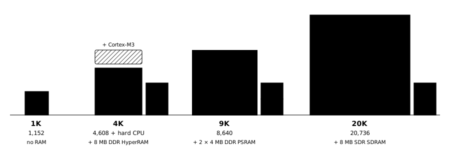
<h2 id="the-tang-nano-family">The Tang Nano family</h2>

<p>Sipeed’s Tang Nano boards put a Gowin FPGA on a board the size of a stick of gum, with a USB-C port for programming the FPGA and various other connectors depending on the model. The four boards span almost a factor of twenty in logic:</p>

<figure class="wide"><img src="/assets/m9b/tang-nano-family.svg" alt="The four Tang Nano boards drawn as squares whose area is their number of lookup tables, each with the RAM in its package" /><figcaption>Each square's area is the board's count of 4-input lookup tables (LUT4); the yellow boxes are the RAM dies in each package, drawn the same size since each board has 8 MB, split in two on the 9K. The 4K's Cortex-M3 is a hard core: it sits next to the logic rather than in it.</figcaption></figure>

<div class="table-wrap">
  <table>
    <thead>
      <tr>
        <th>Board</th>
        <th>FPGA</th>
        <th class="n">LUT4</th>
        <th class="n">Block RAM</th>
        <th>RAM in package</th>
        <th>Hard CPU</th>
      </tr>
    </thead>
    <tbody>
      <tr>
        <td>Tang Nano 1K</td>
        <td>GW1NZ-1</td>
        <td class="n">1,152</td>
        <td class="n">8 KB</td>
        <td>none</td>
        <td>no</td>
      </tr>
      <tr>
        <td>Tang Nano 4K</td>
        <td>GW1NSR-4C</td>
        <td class="n">4,608</td>
        <td class="n">20 KB</td>
        <td>8 MB HyperRAM</td>
        <td>Cortex-M3</td>
      </tr>
      <tr class="hl">
        <td>Tang Nano 9K</td>
        <td>GW1NR-9</td>
        <td class="n">8,640</td>
        <td class="n">52 KB</td>
        <td>8 MB PSRAM (2 dies)</td>
        <td>no</td>
      </tr>
      <tr>
        <td>Tang Nano 20K</td>
        <td>GW2AR-18</td>
        <td class="n">20,736</td>
        <td class="n">92 KB</td>
        <td>8 MB SDRAM</td>
        <td>no</td>
      </tr>
    </tbody>
    <caption>Block RAM counted as 2 KB per block, without the parity bits.</caption>
  </table>
</div>

<p>The 20K is where most retro-computing on Tang Nano boards happens: there’s quite a few cores out there. The 1K is enough for a small CPU, but not for a computer around it, and it lacks the HDMI connector of the other boards in the series. The 4K has a Cortex-M3 built into the silicon, which would be a great base for a small computer system, but the way its address bus is handled makes it tricky to use - I’ll likely write more about this one later.</p>

<p>The 9K has no hard CPU. If there’s going to be a processor, it has to be built from the same 8,640 cells as everything else. That’s the challenge I picked, with a few non-negotiables to start with:</p>

<ol>
  <li><strong>No extra processing.</strong> While it would be tempting to bind in the BL702 by reflashing it, that’s not going to happen here. It’s only the FPGA.</li>
  <li><strong>A generic computer.</strong> The games are test cases, and I don’t want to design specific hardware accelerators for any one of them.</li>
  <li><strong>Real input and output.</strong> HDMI with sound, USB keyboards and mice, an SD card with a real file system.</li>
  <li><strong>Port the software, don’t rewrite it.</strong> Use the C/C++ source code that’s out there and port to the board. Some optimization is acceptable, but the game should look, sound and interact exactly like the original.</li>
</ol>

<p>And that’s it. The baseline would be to just kick off <a href="https://github.com/enjoy-digital/litex">LiteX</a> and generate a baseline system, since it supports this board, but the performance of the result is sadly kind of terrible (at least at the time of writing).</p>

<h2 id="three-dies-in-one-package">Three dies in one package</h2>

<p>The chip on the board, a GW1NR-LV9QN88P, is really three dies in one package: the FPGA itself, and two 32 Mbit PSRAMs (4 MB each). Each PSRAM has its own 8-bit, double-data-rate bus to the FPGA, rated up to 166 MHz. None of those wires leave the package; on the board, the chip looks like any other 88-pin FPGA.</p>

<figure><img src="/assets/m9b/gw1nr9-package.svg" alt="The GW1NR-9 package: the FPGA die and two PSRAM dies, each on its own bus" /><figcaption>The two PSRAM dies sit on separate buses, so they can transfer at the same time. m9b runs both at 144 MHz, in lockstep.</figcaption></figure>

<div class="stats"><div class="stat"><b>8,640</b><span>4-input lookup tables</span></div><div class="stat"><b>52 KB</b><span>block RAM, in 26 blocks of 2 KB</span></div><div class="stat"><b>8 MB</b><span>PSRAM on two dies</span></div><div class="stat"><b>664 MB/s</b><span>PSRAM peak on paper: 166 MHz × 2 edges × 2 dies</span></div></div>

<p>Those numbers frame everything else. 52 KB of block RAM is less memory than a typical 1980s home computer had: a single VGA frame as used by our test games, is 320 × 200 bytes, and wouldn’t fit in all 26 blocks put together. So the programs and their data live in the PSRAM, and the block RAM goes to caches and buffers. The PSRAM’s 664 MB/s is a number on paper: <a href="psram/">part 3</a> follows it down to what the CPU actually gets, which is a small fraction.</p>

<p>There’s no dedicated hardware for anything else. The chip has serializers fast enough for HDMI and the RAM, but the encoder is logic. Sound travels inside the HDMI signal, so that’s logic too. The board has no USB host port; the USB sockets are wired straight to I/O pins, and the protocol is handled in logic too.</p>

<h2 id="the-system">The system</h2>

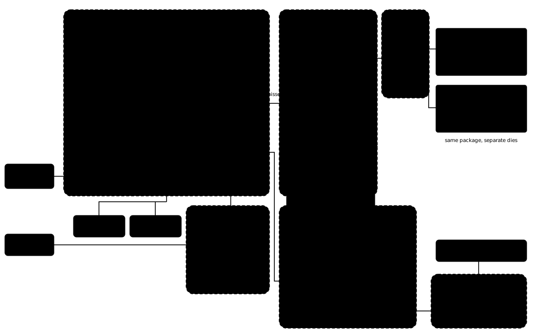
<p>Here is the whole computer, by clock domain.</p>

<figure class="wide"><img src="/assets/m9b/system.svg" alt="m9b system diagram by clock domain" /><figcaption>Dashed regions are clock domains; yellow boxes are block RAM or PSRAM; red boxes are on the board, outside the chip. The bridge and the transfer RAM connect domains: the bridge between the CPU and the controller, which share a clock tree, the transfer RAM between the controller and the video side, which don't.</figcaption></figure>

<p>The top level design is fairly straghtforward. I picked a high performance RISC-V CPU core (vexiiRiscv) and used a good share of the block memory to provide it with ample cache (24 KB of our 52 KB), since the latency of the DDR RAM is pretty scary, and we really don’t want to have to hit it too often. <a href="cpu/">Part 2</a> goes into a lot more detail on the CPU features and subsystem design. The DDR PSRAM controller accesses both dies in lockstep, generating a single command stream that is duplicated to both dies. The PHY is a simple collection of serializers and deserializers. <a href="psram/">Part 3</a> details the inner workings of the controller. The PSRAM controller is also connected to the graphics and audio engine via a transfer RAM, which buffers 2 scanlines of video data and 2 audio buffers. The video engine also has a dedicated RAM for the palette and line table, which can be written directly by the CPU to reduce latency. The HDMI encoder is a simple TMDS encoder that takes the pixel data and generates the HDMI signal. <a href="hdmi/">Part 4</a> looks at this subsystem. The USB host engine is a microcoded core that handles the USB protocol and provides a simple register interface to the CPU. <a href="usb/">Part 5</a> looks at this subsystem. The built-in peripherals are rounded out by a UART for debugging and an SPI interface for talking to the flash chip and SD card.</p>

<h2 id="clocks">Clocks</h2>

<p>All the clocks come from the board’s one 27 MHz crystal, through the chip’s two PLLs and three of its clock dividers. There are a few frequencies we have no control over and that must be respected in order for the system to work: one of these is the dot clock for a VESA standard display mode (in this case 27 MHz for the 720x480 display mode I chose), which also means we need a 5 * 27 = 135 MHz clock for driving the serializers. The other is the 12 MHz clock for USB, which is a standard frequency for full-speed USB. For everything else, we need to use divisors or multiples of these clocks, since we already need both PLLs since 12 and 27 are not integer multiples of each other. I ended up clocking everything off USB clock multiples, with 36 MHz, 72 MHz and 144 MHz clocks for the hardware. Keeping clocks well aligned is very important, since clock domain crossings cost latency.</p>

<figure class="wide" data-link="">
  <svg class="diagram" viewBox="0 0 900 320" role="img" aria-labelledby="clk-t">
    <title id="clk-t">Clock tree: one crystal, two PLLs, three dividers</title>
    <defs>
      <marker id="clk-ah" viewBox="0 0 10 10" refX="9" refY="5" markerWidth="7" markerHeight="7" orient="auto">
        <path d="M0,0 L10,5 L0,10 z" class="arrowhead" />
      </marker>
    </defs>
    <g data-k="osc">
      <rect x="10" y="125" width="110" height="50" rx="6" class="dom d-osc" style="stroke-dasharray: none" />
      <text x="65" y="147" text-anchor="middle" class="t-title">Crystal</text>
      <text x="65" y="165" text-anchor="middle" class="t-freq k-osc">27 MHz</text>
    </g>

    <rect x="190" y="30" width="150" height="70" rx="6" class="box" />
    <text x="265" y="57" text-anchor="middle" class="t-title">pll_hdmi</text>
    <text x="265" y="77" text-anchor="middle" class="t-sub mono">27 × 5</text>

    <rect x="190" y="180" width="150" height="125" rx="6" class="box" />
    <text x="265" y="207" text-anchor="middle" class="t-title">pll_main</text>
    <text x="265" y="227" text-anchor="middle" class="t-sub mono">27 × 16 / 3</text>
    <text x="265" y="247" text-anchor="middle" class="t-small">outputs: ÷1, ÷2, ÷3</text>

    <g class="wire">
      <polyline points="120,150 155,150 155,65 190,65" marker-end="url(#clk-ah)" />
      <polyline points="155,150 155,240 190,240" marker-end="url(#clk-ah)" />
    </g>

    <!-- HDMI branch -->
    <g data-k="pix">
      <line x1="340" y1="65" x2="560" y2="65" class="wire s-pix" style="stroke-width: 2.5" marker-end="url(#clk-ah)" />
      <text x="355" y="57" class="t-freq k-pix">135 MHz</text>
      <text x="540" y="58" text-anchor="end" class="t-small">TMDS serializers</text>
      <polyline points="450,65 450,110 490,110" class="wire s-pix" style="stroke-width: 2.5" />
      <rect x="490" y="95" width="60" height="30" rx="4" class="box" />
      <text x="520" y="115" text-anchor="middle" class="t-sub mono">÷ 5</text>
      <line x1="550" y1="110" x2="620" y2="110" class="wire s-pix" style="stroke-width: 2.5" marker-end="url(#clk-ah)" />
      <text x="630" y="107" class="t-freq k-pix">27 MHz</text>
      <text x="630" y="123" class="t-small">pixels, video engine, HDMI encoder</text>
    </g>

    <!-- main branch -->
    <g data-k="sys">
      <line x1="340" y1="190" x2="560" y2="190" class="wire s-sys" style="stroke-width: 2.5" marker-end="url(#clk-ah)" />
      <text x="355" y="183" class="t-freq k-sys">144 MHz</text>
      <text x="540" y="183" text-anchor="end" class="t-small">PSRAM pins</text>
      <line x1="340" y1="222" x2="560" y2="222" class="wire s-sys" style="stroke-width: 2.5" marker-end="url(#clk-ah)" />
      <text x="355" y="215" class="t-freq k-sys">72 MHz</text>
      <text x="540" y="215" text-anchor="end" class="t-small">PSRAM controller</text>
    </g>
    <g data-k="cpu">
      <polyline points="450,222 450,255 490,255" class="wire s-cpu" style="stroke-width: 2.5" />
      <rect x="490" y="240" width="60" height="30" rx="4" class="box" />
      <text x="520" y="260" text-anchor="middle" class="t-sub mono">÷ 2</text>
      <line x1="550" y1="255" x2="620" y2="255" class="wire s-cpu" style="stroke-width: 2.5" marker-end="url(#clk-ah)" />
      <text x="630" y="252" class="t-freq k-cpu">36 MHz</text>
      <text x="630" y="268" class="t-small">CPU, caches, I/O</text>
    </g>
    <g data-k="usb">
      <line x1="340" y1="292" x2="490" y2="292" class="wire s-usb" style="stroke-width: 2.5" />
      <text x="355" y="285" class="t-freq k-usb">48 MHz</text>
      <rect x="490" y="277" width="60" height="30" rx="4" class="box" />
      <text x="520" y="297" text-anchor="middle" class="t-sub mono">÷ 4</text>
      <line x1="550" y1="292" x2="620" y2="292" class="wire s-usb" style="stroke-width: 2.5" marker-end="url(#clk-ah)" />
      <text x="630" y="289" class="t-freq k-usb">12 MHz</text>
      <text x="630" y="305" class="t-small">USB host engine</text>
    </g>
  </svg>
  <figcaption>The ÷ boxes are the chip's hard clock dividers (CLKDIV). The CPU's 36 MHz is divided from the
    controller's 72, so the two are synchronous.</figcaption>
</figure>

<div class="table-wrap" data-link="">
  <table>
    <thead>
      <tr>
        <th>Clock</th>
        <th class="n">MHz</th>
        <th>Made by</th>
        <th>Why that number</th>
      </tr>
    </thead>
    <tbody>
      <tr data-k="pix">
        <td>TMDS bit clock</td>
        <td class="n">135</td>
        <td>pll_hdmi: 27 × 5</td>
        <td>HDMI sends 10 bits per pixel per channel: 270 Mbit/s, on both edges of 135 MHz</td>
      </tr>
      <tr data-k="pix">
        <td>Pixel clock</td>
        <td class="n">27</td>
        <td>135 ÷ 5</td>
        <td>720 × 480 at 59.94 Hz is a 27 MHz mode. Divided from the bit clock so the serializers' two clocks are in
          phase by construction</td>
      </tr>
      <tr data-k="sys">
        <td>PSRAM I/O</td>
        <td class="n">144</td>
        <td>pll_main: 27 × 16 ÷ 3</td>
        <td>Rated 166 MHz; 144 is the fastest that also divides into 48 for USB</td>
      </tr>
      <tr data-k="sys">
        <td>PSRAM controller</td>
        <td class="n">72</td>
        <td>pll_main ÷ 2</td>
        <td>The I/O serializers take 4 bits per pin per controller cycle</td>
      </tr>
      <tr data-k="cpu">
        <td>CPU</td>
        <td class="n">36</td>
        <td>72 ÷ 2</td>
        <td>As fast as the CPU closes timing (37.8 MHz at the last build), and synchronous with the controller</td>
      </tr>
      <tr data-k="usb">
        <td>USB</td>
        <td class="n">12</td>
        <td>pll_main ÷ 3, then ÷ 4</td>
        <td>Low-speed USB is 1.5 Mbit/s, sampled 8 times per bit: exactly 12 MHz</td>
      </tr>
    </tbody>
  </table>
</div>

<h2 id="where-the-cells-go">Where the cells go</h2>

<p>After place and route, the design uses <strong>7,560 of the 8,640</strong> logic cells (88%) and <strong>25 of the 26</strong> block RAMs. The tighter limit is actually the slices: logic cells are packed in pairs, and 97% of those pairs are in use. At that fill level, the clock speed a build reaches depends heavily on where the tools happen to place things, and every build ends with a look at the timing report.</p>

<div class="table-wrap">

  <table>
    <thead>
      <tr>
        <th>Block</th>
        <th style="text-align: right">Logic cells</th>
        <th style="text-align: right">Block RAMs</th>
        <th>What the block RAM holds</th>
      </tr>
    </thead>
    <tbody>
      <tr>
        <td>CPU (with its caches)</td>
        <td style="text-align: right">≈ 4,340</td>
        <td style="text-align: right">18</td>
        <td>data L1: 8<br />data L1 tags: 2<br />fetch L1: 4<br />fetch L1 tags: 1<br />branch predictor: 1<br />registers: 2</td>
      </tr>
      <tr>
        <td>HDMI encoder</td>
        <td style="text-align: right">≈ 630</td>
        <td style="text-align: right">–</td>
        <td> </td>
      </tr>
      <tr>
        <td>Video engine, video RAM</td>
        <td style="text-align: right">≈ 490</td>
        <td style="text-align: right">2 + 4</td>
        <td>palette and line table: 2<br />transfer RAM (line buffers, audio): 4</td>
      </tr>
      <tr>
        <td>PSRAM controller, bridge</td>
        <td style="text-align: right">≈ 560</td>
        <td style="text-align: right">–</td>
        <td>the bridge’s line buffers are LUT RAM</td>
      </tr>
      <tr>
        <td>USB host, two ports</td>
        <td style="text-align: right">≈ 490</td>
        <td style="text-align: right">1</td>
        <td>the microcode ROM</td>
      </tr>
      <tr>
        <td>UART, SPI, flash reader</td>
        <td style="text-align: right">≈ 270</td>
        <td style="text-align: right">–</td>
        <td> </td>
      </tr>
      <tr>
        <td>Glue: I/O decode, clock crossings, resets</td>
        <td style="text-align: right">≈ 690</td>
        <td style="text-align: right">–</td>
        <td> </td>
      </tr>
    </tbody>
  </table>

  <p class="table-caption">Per-block numbers come from synthesis and are approximate: place and route optimizes across blocks, and its total is the 7,560.</p>

</div>

<p>More than half the chip is the CPU. Everything else is about as compact as I could get it, and I sacrificed features that were not immediately useful along the way. For example, the first versions had a hardware text mode, and that got trimmed off (which also lef to a better looking proportional font on the startup screen). I also trimmed out all forms of audio synthesis, keeping only a simple wave audio out.</p>

<h2 id="the-rest-of-the-series">The rest of the series</h2>

<ol start="2">
  <li><a href="cpu/"><strong>The CPU</strong></a>: why VexiiRiscv, and what every option costs and buys: the caches, the branch predictor, the extensions that fit and the ones that didn’t, 24-bit addresses, and a block RAM bug that shaped the data cache.</li>
  <li><a href="psram/"><strong>The PSRAM controller</strong></a>: two dies driven as one 16-bit memory, the bridge to the CPU, and where 664 MB/s goes.</li>
  <li><a href="hdmi/"><strong>HDMI</strong></a>: the encoder, a video engine built around a line table, and sound in the blanking periods.</li>
  <li><a href="usb/"><strong>USB</strong></a>: a USB host from bare pins, one microcoded engine shared by two ports, and why two resistors matter.</li>
  <li><a href="games/"><strong>The games</strong></a>: porting five 1990s PC games to a machine slower than the PCs they were written for, and what each needed.</li>
</ol>

<p>The source, the RTL and the game ports, is on GitHub: <a href="https://github.com/the-parts-bin/m9b-system">m9b-system</a> ties together the SoC (<a href="https://github.com/the-parts-bin/m9b-core">m9b-core</a>) and the game ports, each a repository of its own.</p>

<h2 id="credits">Credits</h2>

<p>m9b stands on a lot of other people’s work. Each repository’s README lists exactly what it uses, at which version, and what was changed.</p>

<p>The hardware and its firmware:</p>

<ul>
  <li><a href="https://github.com/SpinalHDL/VexiiRiscv">SpinalHDL/VexiiRiscv</a> (Charles Papon): the CPU, built from <a href="https://github.com/the-parts-bin/m9b-VexiiRiscv/tree/m9b">a fork</a> with m9b’s options</li>
  <li><a href="https://github.com/hdl-util/hdmi">hdl-util/hdmi</a> (Sameer Puri): the HDMI encoder, with audio</li>
  <li><a href="https://github.com/nand2mario/usb_hid_host">nand2mario/usb_hid_host</a> (based on hi631’s work): the USB host</li>
  <li><a href="https://elm-chan.org/fsw/ff/">FatFs</a> (ChaN): the FAT file system on the SD card</li>
  <li><a href="https://github.com/picolibc/picolibc">picolibc</a>: the C library, and the programs’ linker script</li>
  <li><a href="https://github.com/Wohlstand/libADLMIDI">Wohlstand/libADLMIDI</a>: the OPL3 emulation the music is rendered with, on the PC</li>
</ul>]]></content><author><name>The Parts Bin</name></author><summary type="html"><![CDATA[A RISC-V computer with caches, 8 MB of PSRAM, HDMI with sound, two USB ports and an SD card, built in the 8,640 lookup tables of a Tang Nano 9K, running Doom, Descent, Tyrian, System Shock and Ultima VII.]]></summary></entry></feed>